PCB or Printed circuit board consists of a board made from non-conductive material on which wires and chips are assembled. PCB is a man-made compound which is highly used in the electronic items these days. Whether it is a digital camera, computer, a music player, a mobile phone or any other electronic device, from the simple devices to complex designs or bio engineering machineries, PCB is sure to be an integral component. Well-designed and well structure of PCB is required and essential for the electronic equipments.
When it comes to the process of printed circuit board manufacturing, keep in mind that executing the creation of board you need to follow certain steps:
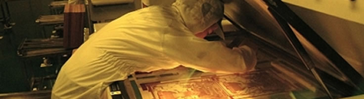
PCB manufacturer china has to make every second detail in manufacturing PCB.
- Setting up the system:- This is the first step of the process, it can really be very difficult for you if not done in a proper way. Therefore, you need to take care of some important things such as process, material required, customer specifications, and above all customer satisfaction.
- Modeling/etching:- Etching doesn’t really mean engraving, but has some connection with it. In this, copper and other unprotected areas are exposed by the etch resist film in order to remove the unprotected copper. This way, the protected copper pads and traces are left in the place.
- Engraving:- A photo mask is combined with chemical etching as to subtract the copper areas from the printed boards.
- Multilayer pressing:- In this, aligning of conductive copper and insulating dielectric layers just to form a solid board material.
- Drilling:- as the name suggests, this involves drilling of holes and the information is stored on the location where the hole is supposed to be drilled.
- Masking:- In this, a protected layer is applied over the copper which has a thin layer of solder mask and copper traces around it.
- Carving:- In the next to final step, the pad areas are coated with a thin solder layer in order to prepare the board for wave soldering.
- Electrical testing:-In final step, check the continuity or shorted PCB manufacturing connections. For doing this, you need to apply voltage between the points.
PCB manufacturer china has to make every second detail in manufacturing PCB.
 RSS Feed